
Read the full paper: arxiv.org/abs/2602.02255
Get a quick overview in this well-written blog: quantumzeitgeist.com/quantum-supe...
23.02.2026 16:09
👍 0
🔁 0
💬 0
📌 0
Read the full paper: arxiv.org/abs/2602.02255
Get a quick overview in this well-written blog: quantumzeitgeist.com/quantum-supe...

Scanning SQUID measurements on a Nb grid
Researchers captured high-res images of phase coherence in superconductors, visualizing quantum “checkerboard” currents with a scanning SQUID. Using a continuous Nb grid made on our MLA 150 Maskless Aligner, they reveal long-range order in Josephson arrays—and how it fragments under magnetic fields.
Read the full paper here: www.nature.com/articles/s41...

Artificial muscles powered by ultrasound? Researchers at ETH Zürich demonstrate programmable microbubble-based muscles with ultrafast (<100 ms) motion and bio-inspired versatility. A DWL 2000 from Heidelberg Instruments enabled the high-precision photomasks behind this breakthrough. #SoftRobotics

A New Hero for Advanced Packaging!
Beyond monolithic chips, we face die shift & warpage. Static photomasks fail in Heterogeneous Integration.
Maskless Lithography is the 'licensed to align' secret weapon needed to save next-gen packages! 🍸
Read more: heidelberg-instruments.com/next-gen-adv...
Great to see 3D additive manufacturing meet precise #CMOS processes! With the help of the MLA 150, a team at Georgia Tech created a hybrid #MEMS force sensor with 3D-printed pillars on silicon piezoresistors – resolving forces down to 20-35 nN. 📖 dx.doi.org/10.2139/ssrn...
@gtresearch.bsky.social

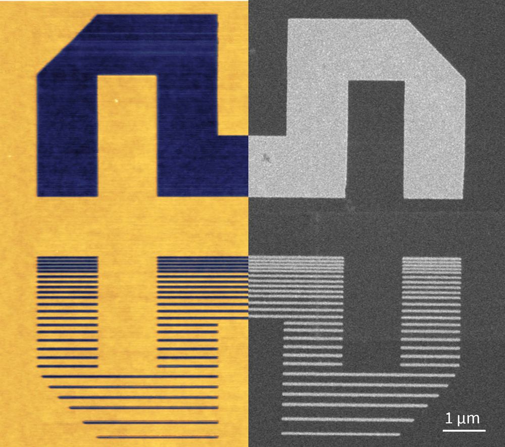
Explore how Nurten Koc’s award-winning silicon metalens was made with the DWL 66⁺ Laser Lithography System: 250 nm gaps, high aspect ratios, low-temp patterning, and scalable fabrication for mid-IR flat optics.
👉 heidelberg-instruments.com/wp-content/u...
#FlatOptics #Metalens #Nanofabrication

🔬 Save the date: #NMLS 2026
Join Nanoscribe, @himt-lithography.bsky.social, GenISys and micro resist technology at DTU Nanolab in Denmark for two days of insights and exchange in nano- and microfabrication.
📅 January 27–28, 2026
Register now for free 👉 tinyurl.com/yzu3kdeb

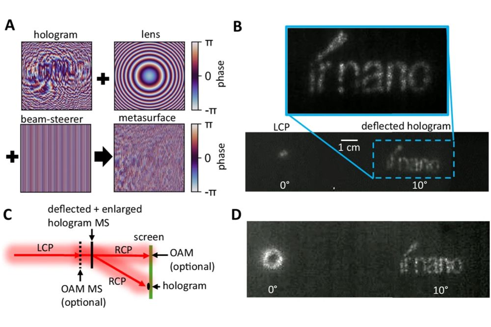
Breakthrough in optical sensing! 💡
Researchers at the Univ. of Adelaide used our MLA 150 & @nanoscribe.com’s GT+ to create micro spiral phase plates that shape light with extreme precision - enabling ultra-sensitive refractive index measurements.
📖 arxiv.org/pdf/2508.19521
#MicroOptics #Photonics

🎉 Celebrating 10 years of the MLA 150!
Since 2015, it’s transformed cleanrooms worldwide, making lithography accessible, flexible & maskless.
Join us to explore its story & enter our anniversary contest to win one of four exciting prizes! 🔗 heidelberg-instruments.com/mla-150-anni...
Ready for Lift-Off? 🛫
Just released a new application note introducing the #NanoFrazor High-Resolution Lift-Off Process - and the results are astonishing!
Ideal for cutting-edge applications in #nanoelectronics, #photonics, and #quantum computing.
👉 heidelberg-instruments.com/wp-content/u...
𝗙𝗿𝗼𝗺 𝗧𝗮𝗯𝗹𝗲𝘁𝗼𝗽 𝘁𝗼 𝗗𝗼𝘂𝗯𝗹𝗲 𝗚𝗮𝗿𝗮𝗴𝗲 𝗗𝗼𝗼𝗿
Every great technological leap starts with a single, precise mark. The question is, how big is your canvas?
At Heidelberg Instruments, we support your vision at every scale. Our portfolio ranges from nanoscale prototyping to huge industrial production tools.
Faster. Simpler. Smarter.
#Metasurfaces are revolutionizing #optics, especially in the infrared spectrum. But traditional fabrication methods are slow, complex, and expensive.
Our new blog post explores how Direct Laser Writing is changing that: heidelberg-instruments.com/direct-laser...
#photonics
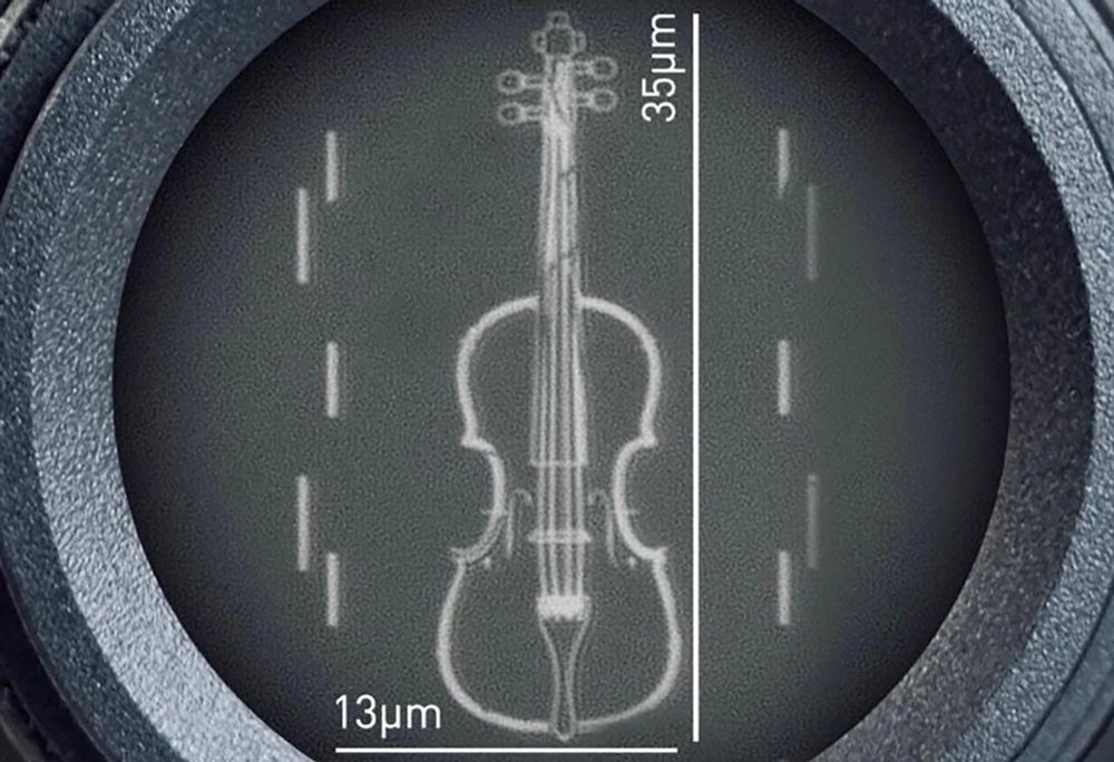
Loughborough University's 'smallest violin' (35x13μm!) 🎻 – a playful yet powerful demo of our NanoFrazor's capabilities for cutting-edge materials research & next-gen computing. Congrats to the team! 👉 heidelberg-instruments.com/loughborough...
@lborouniversity.bsky.social
#nanolithography
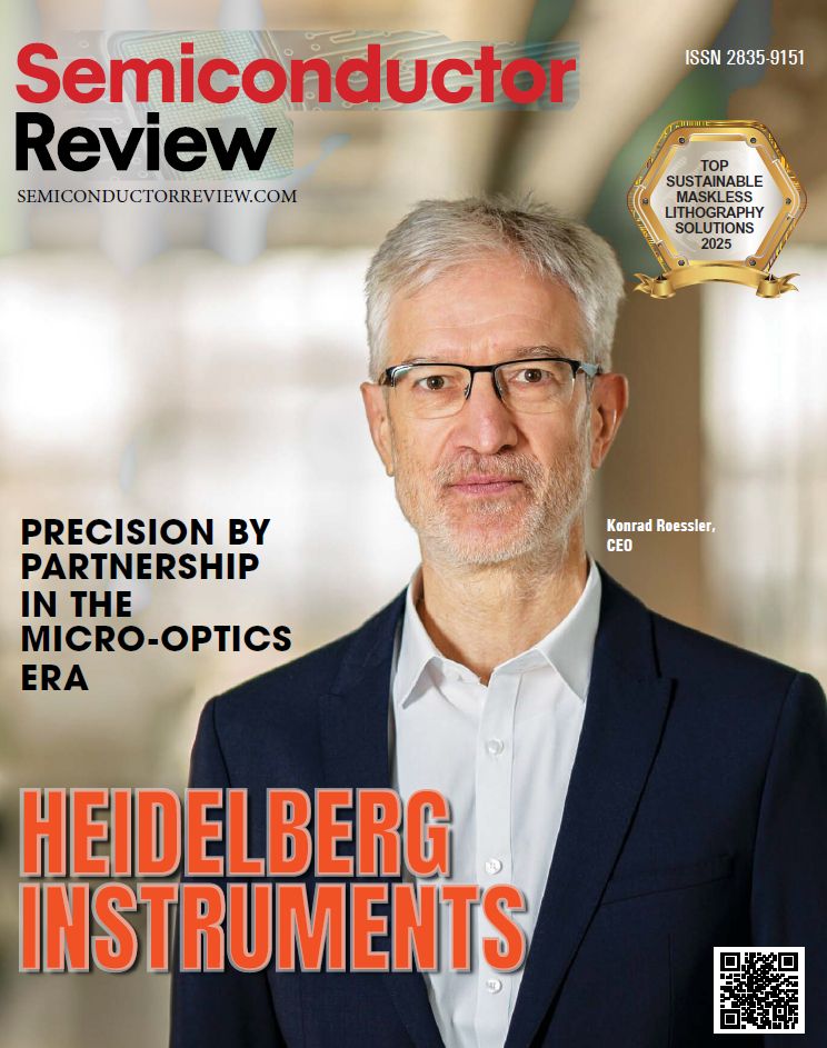
We've been featured in the cover story by Semiconductor Review, highlighting our four decades of leadership in high-precision laser lithography systems and our customer-centric approach. Learn more about our journey: heidelberg-instruments.com/wp-content/u...
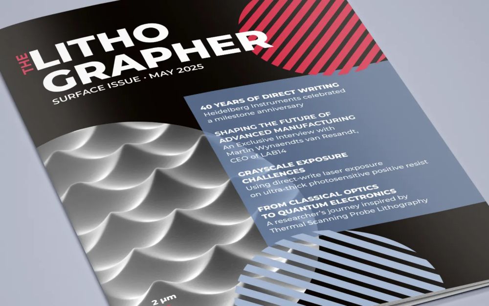
The new Surface Issue of The Lithographer magazine is out! Dive into micro- and nanofabrication, featuring exclusive interviews, insights on grayscale lithography with ultra-thick resists, X-ray optics, quantum electronics, and #BEAMER for photonics.
👉 heidelberg-instruments.com/the-lithogra...
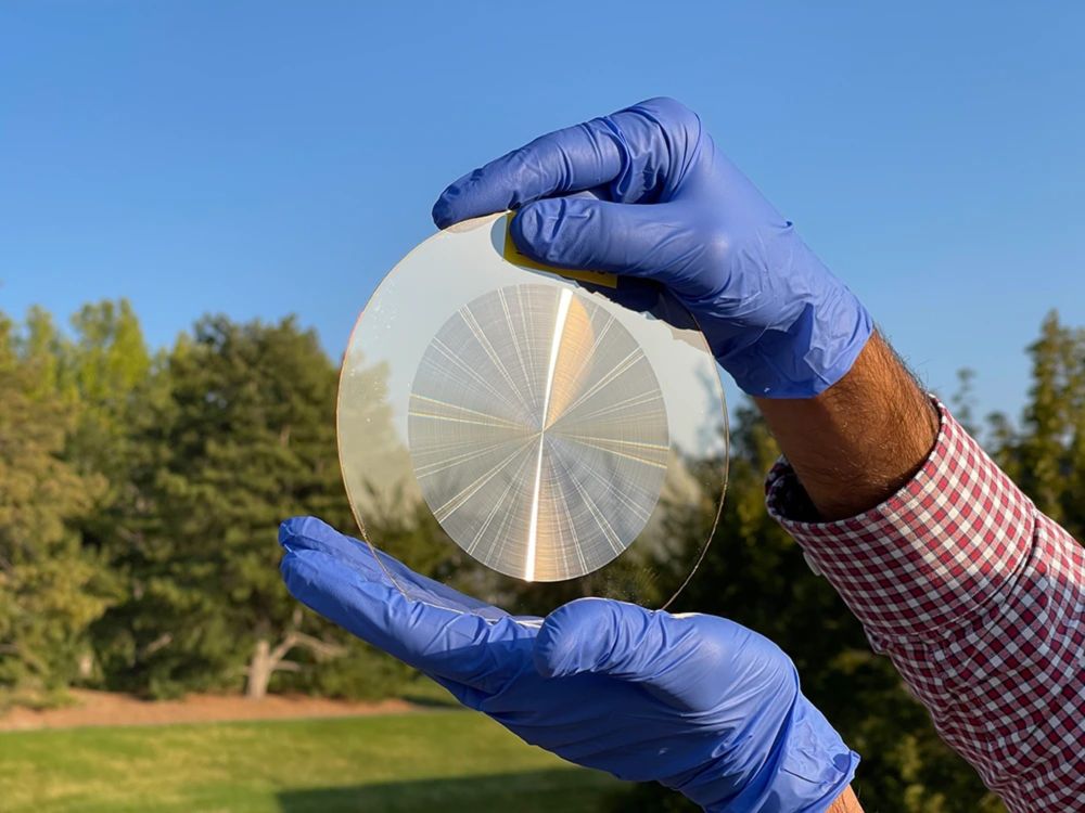
🔭 A flat lens for #space? Yes, really.
10,000 concentric rings, nanometer precision—fabricated with our DWL 66+.
Congrats to Rajesh Menon’s team @utah.edu on pushing the limits of astrophotography.
More: heidelberg-instruments.com/a-new-vision...
#optics #photonics #lithography #microfabrication

